In this lab, you will be implementing a circuit in VHDL that calculates Fibonacci numbers. Here is the pseudocode that describes the behavior of the circuit:
Input: n (specifies that the Fibonacci number to be calculated)
Output: result (the nth Fibonacci number)

i = 3;
x = 1;
y = 1;
while (i <= n)
{
  temp = x+y;
  x = y;
  y = temp;
  i ++;
}
result = y;
You will turnin in your project using e-learning. You should submit both the
code and a screenshot of a working simulation. Please do not turn in ISE
files, only vhd files are necessary.
In this part of the lab, you will implement a controller and datapath in VHDL
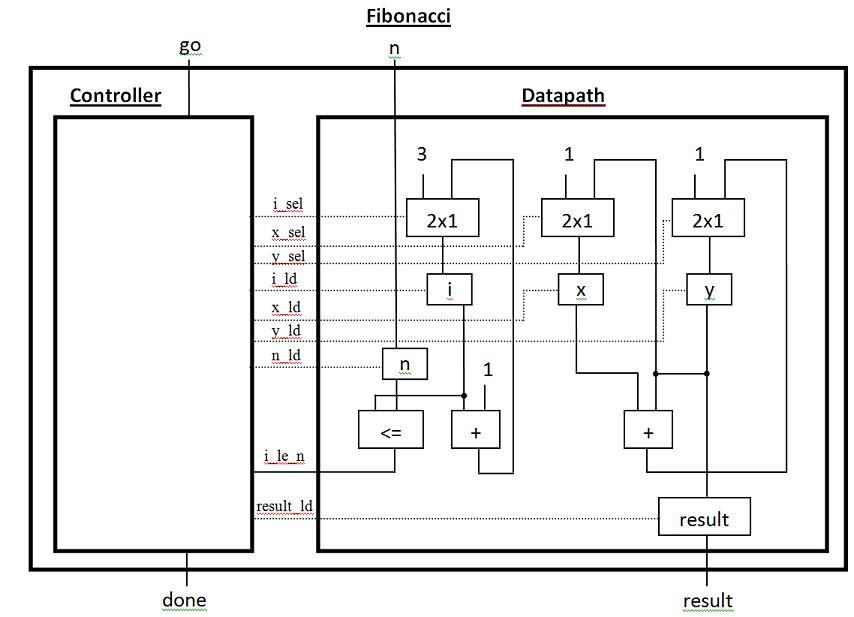
to implement the functionality of the code shown above. A block diagram of the
circuit is shown below:
The circuit has 4 inputs: go, n (8-bit), and clock/reset (not shown). There are also 2 outputs: done and result (8-bit). The circuit should initially wait until go is asserted (active high), and then read in input n, control the datapath as needed to generate the nth fibonacci number, and then store the result in the result register that is connected to the output result. After a result has been generated, done should be asserted (active high) until go is set back to 0 and then reasserted (i.e., until the circuit starts again). The circuit should not start calculating another number until go is reset to 0 and then set to 1.
For the <= entity, use the UNSIGNED type. See the previous tutorials for examples of how to use UNSIGNED. For all other signals, use the STD_LOGIC or STD_LOGIC_VECTOR type.
The dotted lines between the controller and datapath represent control signals need to control the functionality of the datapath. The control lines for the muxes handle selecting the appropriate input. The control lines for the register specify when values should be loaded. The solid line i_le_n is an output from the datapath that the controller uses to determine if the code has completed.
Your project should have the following entities, implemented in the specified way:
Note: You can ignore invalid values of n, such as values < 1 or values that result in overflow from the 8-bit registers.
In this part of the lab, you will implement another circuit for the same pseudocode, but this time using an FSMD as explained in class. The main difference here is that you are not explicity specifying the datapath, and instead are specifying operations that are executed during each stage of the FSM.
For part 2, you will only need 2 entities:
Synthesize the circuits from part 1 and part2 using ISE, and compare their areas. Use any device you want as a target, and compare the area using slices. Explain the difference in area, if any.